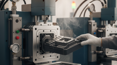
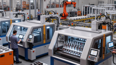
Electronics are becoming smaller, lighter, and more exposed to daily handling. A connector may face vibration, moisture, and repeated cable movement. Traditional molding can protect these parts, but excessive pressure may stress delicate components. low pressure injection molding offers a gentler alternative for sensitive electronic assemblies. It surrounds components with molten polymer at controlled pressure. This approach can reduce mechanical strain around solder joints, wires, and miniature sensors. The result is often a cleaner protective layer with fewer design compromises.
From prototype builds to established production lines, engineers use this process for encapsulation and sealing. It can support compact housings, flexible cables, circuit boards, and sensor modules. Material choice remains critical. Thermoplastics, hot-melt compounds, and reactive materials behave differently during filling and cooling. Qualified teams review viscosity, temperature limits, adhesion, and moisture resistance before production. Process data also matters. Pressure, injection speed, and curing conditions should be recorded and checked. Small changes can affect coverage.
Still, low pressure injection molding is not a universal solution. Some products require higher structural strength or specialized thermal performance. Complex geometries may also demand additional tooling analysis. A reliable decision combines laboratory testing, supplier experience, and application-specific validation. Teams should inspect cross-sections, test electrical insulation, and evaluate aging under realistic conditions. A supplier’s documented process controls can strengthen confidence. The most valuable benefit is not simply lower pressure. It is better protection with less mechanical disturbance. Yet, every design deserves a careful challenge. Could the material fail after years of heat, bending, or humidity? That question keeps the process honest.
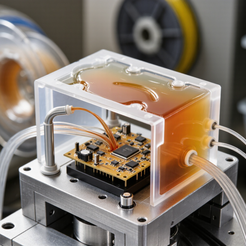
Low pressure injection molding is a protective process for sensitive electronic assemblies. A heated, low-viscosity thermoplastic material flows around a circuit board at relatively low pressure, often below 40 bar. It cools into a flexible seal around connectors, sensors, wires, and solder joints. Unlike rigid epoxy potting, the material can reduce stress during thermal expansion and contraction. It also creates a barrier against moisture, dust, vibration, and accidental contact.
The method fits growing electronics production. Mordor Intelligence estimated the electronics manufacturing services market at about USD 856.7 billion in 2024. More devices also create more lifecycle pressure. The Global E-waste Monitor 2024 recorded 62 billion kilograms of electronic waste in 2022, while only 22.3% was formally collected and recycled. Reworkable thermoplastic compounds may support easier repair than permanent encapsulants, but this depends on the material and product design.
A practical detail matters. Mold temperature, injection speed, and venting must match each component. Too much heat can damage plastics or batteries. Too little heat can leave voids. In production trials, a narrow process window may appear acceptable at first. It may fail after humidity testing.
Not a magic shield. Engineers still need insulation testing, thermal cycling, adhesion checks, and controlled material traceability. The best design balances protection, serviceability, cycle time, and actual field conditions.
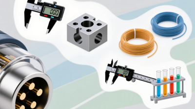
Low pressure injection molding protects delicate electronic assemblies with controlled pressure and flexible encapsulation. The process usually begins with cleaning and drying the circuit board, cable, sensor, or connector. Moisture must be removed. Otherwise, trapped vapor can create bubbles or weak seals.
The operator places the component inside a shaped mold and closes it gently. A thermoplastic sealing material is heated until it flows. Injection pressure commonly ranges from 5 to 40 bar, reducing stress on solder joints and miniature components. The material surrounds wires and housings, then cools into a resilient protective layer.
This barrier can resist dust, vibration, moisture, and repeated temperature changes. Cycle time depends on material, mold design, and part thickness. Practical trials matter more than optimistic datasheets.
A 2024 Grand View Research report estimates the global electronics manufacturing services market will expand at about 7.5% annually through 2030. That growth increases pressure for reliable, scalable protection methods. Low pressure molding can support automated production while reducing secondary sealing steps.
However, it is not automatically the best answer. Poor venting, uneven heating, or incompatible materials can still cause defects. I have seen small mold gaps create visible flash and incomplete coverage. Design reviews should examine cable movement, thermal expansion, repair needs, and end-use temperature ranges before production approval.
Low pressure injection molding offers a controlled way to protect sensitive electronic components without forcing resin into delicate areas. During production, the material flows gently around circuit boards, wires, sensors, and miniature connectors. This lower mechanical load can reduce component movement, cracked solder joints, and deformation near seals. The result is practical protection against moisture, dust, vibration, and accidental handling.
Better enclosure performance.
Key benefits appear when reliability and compact design must coexist. Encapsulation can create strain relief around cable exits and consistent insulation around exposed conductors. It may also replace several mechanical parts, reducing assembly steps and potential leak paths. Engineers can select compounds for flexibility, temperature range, flame behavior, and electrical insulation.
Material testing remains essential. A resin that performs well on paper may bond poorly to a coating or connector surface.
In a sound qualification process, teams inspect fill coverage, adhesion, voids, curing, and dimensional stability. They should test samples through thermal cycling, humidity exposure, vibration, and pull-force checks. These tests reveal weaknesses that visual inspection misses.
Low pressure does not mean low risk. Poor venting can trap air, while excessive heat can damage nearby components. I would not approve a design from molding trials alone; field conditions often expose overlooked tolerances. Pilot runs, traceable process records, and honest failure review make the protection more dependable.
Low-pressure injection molding protects electronic assemblies with less mechanical stress than conventional high-pressure molding. That difference matters around ceramic capacitors, fine-pitch connectors, and thin solder joints. A 2024 Global E-waste Monitor report recorded 62 million tonnes of electronic waste in 2022, while only 22.3% entered documented recycling channels. Material selection should therefore consider service life, repair access, and end-of-life separation—not only initial cost.
Thermoplastic hot-melt compounds can provide strong adhesion and fast processing. Polyamide offers toughness, while polyolefin materials often provide better moisture resistance and flexibility. TPU can suit flexible cable transitions, but it may absorb more moisture than expected.
Check the technical data sheet at the actual operating temperature. Dielectric strength, glass-transition temperature, water absorption, shrinkage, and flame performance require testing on the finished assembly. UL 94 ratings alone do not describe long-term reliability.
Design details decide whether the process succeeds. Leave a controlled flow path around tall components, add vents near the final fill area, and avoid sharp internal corners. A small radius can reduce stress concentration. Keep sensitive connectors accessible when future service matters.
In production reviews, trapped air often causes more trouble than material choice. A glossy overmold can still hide voids. That is easy to miss.
One practical weakness remains: low-pressure molding may improve protection but complicate rework. Designers should test peel strength, thermal cycling, humidity exposure, and connector insertion force before approving the geometry. These checks align with reliability practices described in IPC assembly and packaging guidance.
Low pressure injection molding is useful when electronics need gentle, continuous protection. Molten thermoplastic enters a mold at relatively low pressure and temperature. This reduces stress on delicate solder joints, wires, and miniature sensors. Production reviews often expose problems around connector edges and cable exits. Those areas commonly show gaps, flash, or incomplete sealing.
Typical applications include printed circuit board assemblies, automotive sensors, LED modules, wearable devices, and compact control units. The process can resist splash water, dust, vibration, and repeated handling. It also anchors loose wires inside a shaped protective layer. For a small sensor, that may prevent movement during installation. For a wearable device, soft encapsulation can improve comfort around the housing. Not always.
Limitations deserve equal attention. The molding material must match the component’s temperature, chemical, and electrical requirements. Poor adhesion can create hidden moisture paths. Excessive coverage may trap heat around power components. Repair becomes difficult after encapsulation, especially when a failed board sits deep inside. Complex connectors may need masking, inserts, or secondary sealing. A low-pressure process is not automatically low-risk. Practical testing can reveal failures after thermal cycling, even when initial leak tests pass. That assumption can fail. Engineers should test real assemblies, not only material samples. Warpage, cooling behavior, dimensional tolerances, and rework plans need early review.
| Application or Factor | Typical Electronics Use | Why Low Pressure Injection Molding Is Considered | Common Materials or Design Features | Key Limitations and Risks | Suitability |
|---|---|---|---|---|---|
| Printed Circuit Boards | Protection of populated circuit boards, control modules, and compact electronic assemblies. | Injection pressures are generally much lower than those used in conventional thermoplastic molding, which can reduce mechanical stress on components, solder joints, and delicate interconnects. | Hot-melt polyamides, polyolefins, or other electrically insulating encapsulants; selective encapsulation and overmolding are common. | Heat-sensitive components and moisture trapped during processing may be damaged. Repair and component replacement can become difficult after encapsulation. | High for sealed assemblies |
| Sensors and Sensor Modules | Encapsulation of temperature, pressure, motion, position, and environmental sensor electronics. | Can provide protection from vibration, dust, moisture, and handling while allowing molded material to flow around small components. | Low-viscosity insulating materials, thin-wall cavities, venting features, and openings that preserve the sensing surface. | The encapsulant must not block the sensing element or alter its thermal, pressure, optical, or mechanical response. Material shrinkage can affect calibration. | High with a validated design |
| Connectors and Cable Terminations | Sealing cable exits, strain-relief areas, terminal interfaces, and compact connector assemblies. | Can form a continuous protective layer around wires and terminals while reducing the risk of component displacement during molding. | Flexible or semi-flexible hot melts, molded strain reliefs, cable glands, and integrated sealing lips. | Material compatibility with cable jackets and connector plastics must be verified. Poor adhesion or voids can permit water ingress. | High for sealing and strain relief |
| Coils, Inductors, and Transformers | Insulation and mechanical stabilization of windings, bobbins, and small magnetic components. | Low-pressure filling can reduce the likelihood of winding movement and mechanical damage compared with higher-pressure processes. | Electrically insulating encapsulants with suitable dielectric strength and thermal aging performance. | Air pockets can reduce insulation reliability and heat transfer. Thermal expansion differences may create stress during temperature cycling. | Medium to high |
| LED and Lighting Modules | Protection of LED boards, driver electronics, wiring joints, and compact lighting assemblies. | Supports sealing and electrical insulation in applications exposed to vibration, dust, or occasional moisture. | Optically compatible or opaque encapsulants, heat-resistant formulations, and designs with controlled thermal paths. | Encapsulant discoloration, reduced light output, thermal buildup, and optical distortion may occur if the material is not selected correctly. | Medium to high |
| Automotive Electronic Modules | Protection of small control units, sensors, wiring interfaces, and electronic subassemblies used in vehicles. | Can provide sealing, vibration resistance, and electrical insulation in a relatively compact process. | Automotive-grade encapsulants, reinforced housings, moisture barriers, and controlled bond lines. | Long-term exposure to temperature cycling, fluids, vibration, and electrical loads requires extensive validation. Repairability is limited. | Medium to high |
| Wearable and Portable Electronics | Encapsulation of compact boards, battery contacts, small sensors, and cable interfaces. | Thin, conformal protection can improve resistance to sweat, dust, handling, and incidental moisture without requiring a large enclosure. | Flexible encapsulants, thin-wall designs, molded gaskets, and materials with suitable skin-contact or environmental properties when required. | Battery heat, charging safety, user-repair requirements, and repeated flexing can limit the use of permanent encapsulation. | Medium |
| Power Electronics | Insulation and environmental protection for compact power supplies, terminals, and low-to-moderate power assemblies. | May reduce assembly steps and improve protection against contamination and accidental contact with conductive parts. | High-dielectric-strength materials, flame-retardant grades, and designs that maintain required creepage and clearance distances. | Low-pressure molding is not a substitute for thermal management, insulation coordination, or appropriate high-voltage qualification. Heat dissipation may be restricted. | Medium; application-dependent |
| Moisture and Contamination Protection | Protection against humidity, dust, salt residue, oils, and other contaminants. | A continuous molded barrier can reduce exposed joints, cable openings, and pathways for contamination. | Hydrophobic or chemically resistant encapsulants, overlap joints, sealed interfaces, and controlled venting. | Protection depends on adhesion, coverage, void control, and the permeability of the selected material. No molding process guarantees absolute waterproofing. | High when properly validated |
| Production Efficiency | Repeatable encapsulation of medium- to high-volume electronic assemblies. | Can combine sealing, insulation, strain relief, and mechanical protection in one operation, potentially reducing secondary assembly work. | Reusable molds, automated dispensing or injection equipment, controlled material temperature, and fixture-based positioning. | Tooling, curing or cooling time, material handling, and process qualification can increase initial investment. Cycle time depends strongly on part size and material. | Medium to high |
| Repairability and Rework | Post-production servicing of molded circuit assemblies. | Permanent encapsulation can improve protection during service, but it is generally intended for assemblies that do not require frequent component replacement. | Selective molding, removable covers, service windows, or localized potting where maintenance is necessary. | Fully molded parts are difficult to inspect, repair, or disassemble without damaging the electronics or enclosure. | Low for fully encapsulated products |
| Thermal Management | Protection of electronics that generate heat during operation. | Some encapsulants can stabilize components mechanically and provide a controlled interface around the assembly. | Thermally conductive compounds, heat sinks, thermal interface materials, and vented or mechanically supported designs. | Many low-pressure encapsulants are thermal insulators. Added material can increase thermal resistance and raise component operating temperatures. | Low to medium unless engineered |
| High-Voltage Insulation | Electrical isolation of terminals, splices, and selected high-voltage subassemblies. | Encapsulation can reduce exposure to contaminants and help maintain insulation around complex geometries. | High-dielectric-strength, flame-retardant materials; carefully controlled wall thickness, creepage, and clearance. | Voids, sharp edges, moisture absorption, partial discharge, and inadequate qualification can compromise insulation reliability. | Medium; requires formal testing |